
Design How-to
Reducing EMI in Buck Converters
|
Reducing Electro Magnetic
Interference (EMI) in switch mode power supplies can
be a challenge, because of the very high frequencies
that are involved. Electrical components behave differently
than expected, because the parasitic effects of the
components often play an important role. This feature
story highlights some of the key aspects of EMI in low
voltage buck converters, and provides practical tips
how to reduce EMI in the buck converter design. |
Source of
EMI and how to identify current loops in a Buck converter
|
|
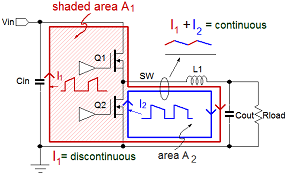
High frequency magnetic
fields are generally the main radiation source in non-isolated
DC/DC buck converters. These fields are generated by
loop currents with high di/dt. The DC/DC buck converter
has two main loops where high frequency currents flow:
I1 when MOSFET Q1 is ON and I2 when Q1 is OFF and Q2
is ON. The input loop (shaded area A1 as shown at right side)
is considered the most critical loop for EMI as its
current is discontinuous, and generates the most high
frequencies.
|
 |
Read more to find out the
basics of EMI
radiation and how to reduce the EMI in area A1.
.png)
|
Design tip
1 : Component choice and Input and output filtering
|
|
All capacitors have
some ESR and ESL, which increases the capacitor impedance
and results in extra voltage drop across the capacitor
at higher frequencies. Smaller size MLCCs have lower
ESL, so using multiple different size MLCC such as 1206
and 0603 or 0402 size capacitors as filter element as
close as possible to converter switching loops can help
reduce the voltage drop due to parasitic elements. Extra
L-C filtering in the input line can be very effective
to reduce conducted differential mode noise. Read more
to find out how to filter input and output stages.
|
Design tip
2 : Reduce converter ringing and switching speed
|
|
Fourier analysis of the switch current waveform helps
to understand the relation between pulse width, rise
and fall times in time domain and the high frequency
harmonic content in frequency domain. Reduction of the
buck converter waveform ringing and switching speed
can help reduce the EMI but will increase switching
losses. Adding a series resistor in bootstrap circuit
will reduce MOSFET switching speed, and adding an RC
snubber or an RL snubber will damp the resonances in
the switching loop, reducing the high frequency content
of the switching signals. Find out more details on how
to add these measures
and practical examples.
|
|
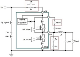 |
Design tip 3 : Examine the layout loops
in detail
|
|
When you find increased radiation levels in certain
areas of your board, it is important to examine the
local (Vin decoupling) current loops in detail. Knowing
component properties like trace inductance, capacitor
ESL and even IC wire bonding scheme can help to understand
the actual size of the critical loop, and by modifying
PCB routing or different placement of capacitors, the
loops may be reduced considerably, which has a great
impact on radiated EMI. Best of all, these solutions
often don't cost extra money if they are implemented
in the early stage of design.
|
|
.jpg) |
Build your own EMI probing tools
|
|
It is possible to do near field EMI measurements in
the lab by using some simple self-made tools: A loop
antenna can help to find the main radiation from current
loops in your application. A high frequency current
probe can measure the common mode current in wiring,
which is an indication of radiation levels. A sniffer
probe can measure high frequency currents in PCB traces
and component pins to identify noise currents. These
probes can be connected to a spectrum analyzer or oscilloscope
to check the noise levels. Read here how to build these
handy tools yourself.
|
|
.jpg) |
Read the full application note “Reducing EMI in Buck converters” for
some theory and many practical examples. |
New Products
|
|
RT9076
is a new generation of cost effective, 25μA Iq,
250mA, 2.5V-6V input, and 1.2V-3.3V fixed output
LDO voltage regulator in a small
SOT-23-3 package, ideal for low BOM cost
LDO applications without Enable.
|
|
|
RT9083
is a new generation of cost effective, 30μA Iq,
1.2V-5.5V input, 0.9V-3.3V fixed
output, 250mA LDO voltage regulator with
enable function in TSOT-23-5 package. Ideal for cost sensitive
general purpose LDO applications.
|
|
|
RT9077
is a 200mA, 3.5V-14V input LDO
voltage regulator with fixed 2.5/3.3/4.2/5/8/9V output voltage
and Enable control in TSOT-23-5
package. Very suitable for low power voltage regulation in
12V supply systems.
|
|
|
RT9079
is a 3.5V-36V input, 50μA Iq,
200mA LDO voltage regulator supporting
2.5V-12V fixed Vout with Enable
in TSOT-23-5 package. It is ideal for low
power voltage regulation in battery-powered and automotive
/ industrial input range applications.
Find more about Richtek
LDO products
|
|
|
RT6217E/F
(500k/800kHz) series are 4.5V-23V input,
3A output current, ACOT®
Synchronous Buck Converter with selectable PSM/PWM
Mode pin in TSOT-23-8 package. The ultra-fast
transient response, and wide input voltage range makes it
an ideal choice for step-down applications running from
5V/12V/19V rails like Set Top Box, TVs, etc.
See other ACOT® products
|
|
|
RT5028D
is an I2C controlled highly-integrated
low-power analog SOC with PMIC in WQFN-56L 7x7
single chip for automotive and industrial applications
like car infotainment and portable POS systems.
Integrating 4 Buck converters (2.4A/2A/1.6A/2A), 8 LDOs
for system power and embedding one user programmable EEPROM
(MTP) for autonomous user defined start-up sequence and
output voltage setting.
|
 |
 |
|
Richtek would like to congratulate all winners who have signed up for My Richtek and won the prize in 2015. Please join
MyRichtek now, a fast way to manage your product subscription, samples and datasheets, and become the next prize winner in 2016. |
|